

CMP Slurry
Category: CMP Pad
Product details
| Product | Description | Category | Feature |
DP53XX DP55XX DP59XX Series | Used for polycrystalline silicon (Poly-Si) removal and planarization in IC manufacturing processes. Features high Poly-Si removal rate, high dilution ratio, and low defectivity. Successfully deployed in high-volume memory device production. | Polycrystalline Silicon Slurry | Solids Content: 4%-20%; Particle Size: 60-200 nm; High Poly/Oxide Removal Selectivity |
DP54XX DP56XX DP58XX Series | Used for silicon nitride (SiN) film removal and planarization in multi-scenario IC manufacturing processes. Offers strong dishing control and precise gate height control. Widely adopted in logic device fabrication. | Silicon Nitride Slurry | Solids Content: 2%-20%; Particle Size: 50-100 nm; Moderate SiN/Oxide Removal Selectivity |
| ZX Series | Used for dielectric material (oxide, OX) removal and planarization in IC manufacturing. Features high removal rate, high dilution ratio, and low defectivity. Deployed in high-volume memory production. | Dielectric Slurry | Solids Content: 3%-20%; Particle Size: 80-150 nm; High OX Film Removal Rate |
| DP6XXX Series | For silicon wafer surface Chemical Mechanical Polishing (CMP) in IC manufacturing. Features high removal rate and low surface defectivity. | Silicon Substrate Slurry | Solids Content: 2%-20%; Particle Size: 50-100 nm; High Si Removal Rate; Low Wafer Defectivity |
| DW6XXX Series | Utilizes proprietary alumina abrasive particles. For tungsten (W) gate material removal and planarization in logic device manufacturing. Features high planarization efficiency, high selectivity, and low defectivity. Deployed in high-volume logic production. | Tungsten Metal Gate (WMG) Slurry | Solids Content: 0.01%-0.3%; Particle Size: 60-120 nm; Customizable W, TiN, OX removal rates; High W/OX Removal Selectivity |
| DW3XXX、DW5XXX Series | Used for tungsten (W) material removal and planarization in IC manufacturing. Offers controllable selectivity (customizable), low defectivity. Deployed in high-volume logic production. | Tungsten (CTW) Slurry | Solids Content: 1%-10%; Particle Size: 60-100 nm; Customizable W, TiN, OX removal rates; Moderate W/OX Removal Selectivity |
| DB Series | Used for barrier layer removal and planarization in copper interconnect processes. Selectively polishes copper and barrier layer. Delivers high planarity, low defectivity, low corrosion, and minimal dishing. | Copper Barrier Slurry | Solids Content: 5~25%; Particle Size: 20-150 nm; Customizable Cu, OX, BD, Ta, TaN, SiN film removal rates |
| DC Series | Used for copper (Cu) metal removal and planarization in IC manufacturing. Features high removal rate, high dilution ratio, and low defectivity. | Copper Slurry | Solids Content: 0.5%-2%; Particle Size: 30-120 nm; High Cu Removal Rate; Low Cu/OX Removal Selectivity |
| ZA Series | Utilizes proprietary alumina abrasive particles. For aluminum (Al) gate material removal and planarization in IC manufacturing. Features high planarization efficiency, high selectivity, and low defectivity. Deployed in logic device fabrication. | Aluminum Gate(HKMG) Slurry | Solids Content: 0.5%-2%; Particle Size: 60-120 nm; Customizable Al, TiN, OX film removal rates; High Al/OX Removal Selectivity |
| DS Series | Utilizes proprietary ceria abrasive particles. For dielectric material (oxide, OX) removal and planarization, including STI (Shallow Trench Isolation) structure formation. Features high OX removal rate, high planarization efficiency, low dishing, and low defectivity. | Ceria Slurry | Solids Content: 0.5%-5%; Particle Size: 80-150 nm; Customizable OX Removal Rate; High OX/SiN Removal Selectivity |
| DLS Series | Abrasive particles --- Core raw material for CMP slurries. Features ultra-low metallic impurity content. Widely used in FEOL processes and demanding metal interconnect processes. Offers low hardness and low wafer defectivity. | Ultra-Pure Silica Abrasive | Solids Content: 15%-21%; Particle Size: 35-180 nm; pH 6.5~8.6; All metallic impurities < 20ppb; Customizable abrasive particle charge |
| DLSB Series | Used for slurry formulation across various IC manufacturing process steps. Provides mechanical abrasion force and chemical component adsorption sites. Suitable for high-speed removal and high selectivity control scenarios. | High-Purity Silica Abrasive | Solids Content: 20-50%; Particle Size: 20~150 nm; pH 8~11; Mohs Hardness ~6 |
Note: Colloidal silica abrasive used unless otherwise specified.
Keywords:CMP Slurry
Previous: CMP Pad
Next: CMP Chemical
CMP Slurry
CMP Slurry is a colloid with uniformly dispersed particles. It can form an oxide film on the surface of silicon wafers, which is then removed by the abrasive particles in the slurry to achieve the polishing effect. Generally, factors such as the flow rate, viscosity, temperature, composition, and pH value of the slurry will affect the removal effect.
Related products
Integrated circuit materials
CMP Pad
-

CMP Pad
CMP Pad is a technology-intensive product that spans multiple disciplines such as polymer chemistry, polymer physics, organic synthesis, fluid mechanics, tribology, and precision machining.
-

CMP Slurry
CMP Slurry is a colloid with uniformly dispersed particles. It can form an oxide film on the surface of silicon wafers, which is then removed by the abrasive particles in the slurry to achieve the polishing effect. Generally, factors such as the flow rate, viscosity, temperature, composition, and pH value of the slurry will affect the removal effect.
-

CMP Chemical
It is mainly used to remove impurities such as dust particles, organic substances, inorganic substances, metal ions, and oxides remaining on the surface of wafers. It meets the extremely high cleanliness requirements of integrated circuit manufacturing and plays an important role in the yield rate of wafer production.
Advanced semiconductor packaging
-

Advanced Packaging PSPI
GHI-line exposure<br> Resolution: 5~10 μm<br> Curing in high/low-temperature<br> Film thickness: 5~15 μm<br> Curing temperature: 200~400 °C<br> Superior mechanical/electrical properties and adhesion to copper
-

Temporary Bonding Adhesive(TBA)
Bonding at room temperature and low stress<br> Excellent high-temperature resistance<br> (withstands long-term exposure to 300°C for > 1.5 hours)<br> Debonding achievable via mechanical or laser methods (248nm/308nm/355nm)
-

Wafer-Level Insulating Passivation Layers
Wafer-Level Passivation Layers (PI/PSPI) are critical materials utilized in Wafer-Level Packaging (WLP) processes. Applied via spin coating and patterned through exposure and development, they form a permanent, patterned protective layer. Following high-temperature curing, these layers provide excellent passivation protection and stress buffering for the chip surface, effectively enhancing device reliability.

Semiconductor display materials
OLED
-
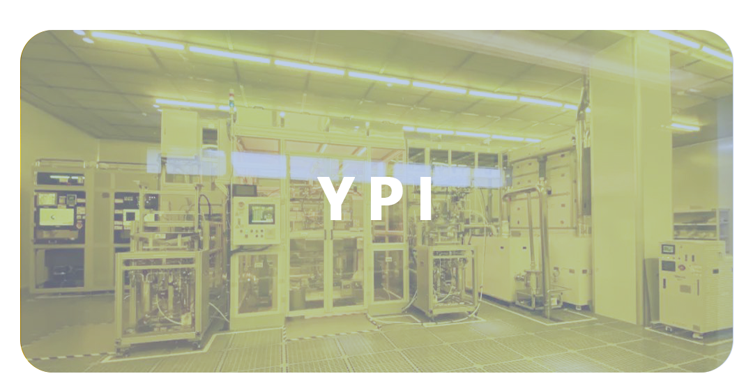
YPI
Viscosity: 4000~7000 cP<br> Nonvolatile matter: 10%~20%<br> Film thickness: 5~15 μm<br> Curing Temperature: 450~480 ℃<br> 1% weight loss temperature: >560 ℃<br> Superior optical/mechanical properties
-
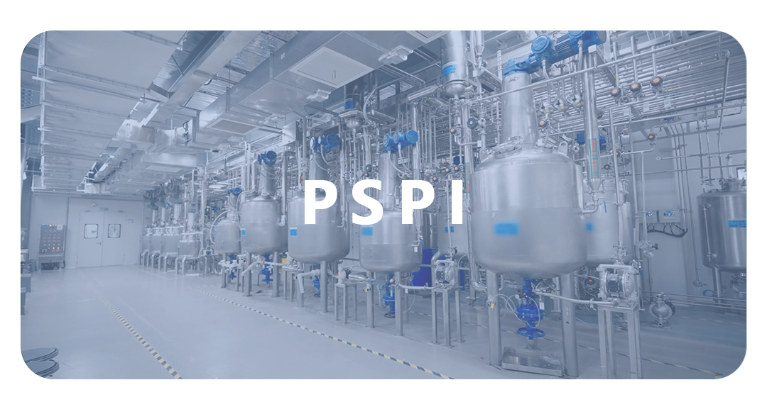
PSPI
GHI-line exposure<br> Resolution: 2~3 μm<br> High/low-sensitivity PSPI<br> Film thickness: 1~5 μm<br> Curing temperature: 250~280 °C<br> Superior optical/mechanical properties
-
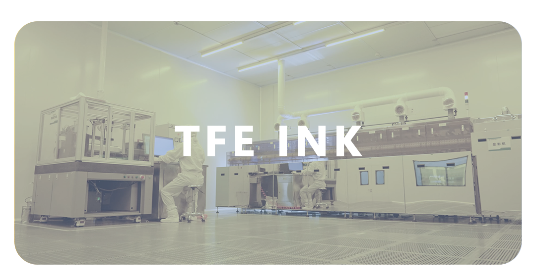
TFE INK
Viscosity: 20~22 cP<br> Water content: <50 ppm<br> UV curing wavelength: 395 nm<br> Film thickness: 6~15 μm<br> Superior optical properties
-
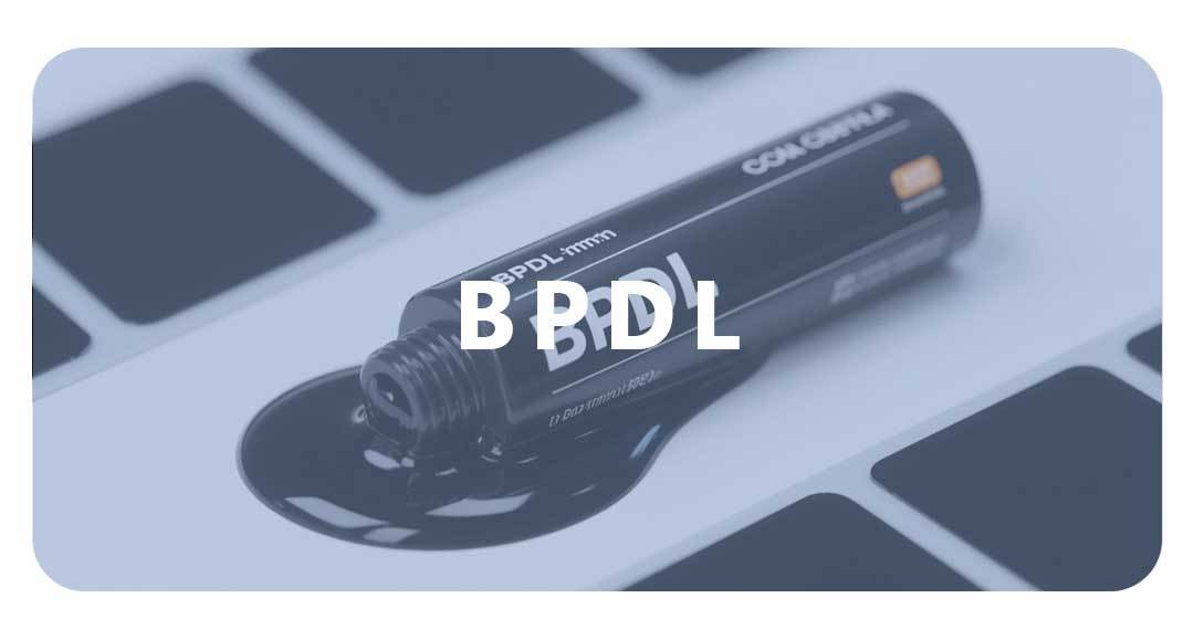
BPDL
Resolution: 5 μm<br> Particle size: 50~70 nm<br> Curing temperature: 250~280 °C<br> Film thickness: 1~5 μm<br> Optical density (OD): >1 /μm
-

PFAS free PSPI
GHI-ine exposure<br> Resolution: 2~3 μm<br> High/low-sensitivity PFAS free PSPI<br> Film thickness: 1~5 μm<br> Curing temperature: 250~280 °C<br> Superior optical/mechanical properties

MICRO-LED
-
PSPI
GHI-ine exposure<br> Resolution: 3 μm<br> Film thickness: 1~5 μm<br> Curing temperature: 250~280 °C<br> multiple curing processes/good adhesion to metal substrates<br> Superior optical/mechanical properties
-

Black Bank
Resolution: 10 μm<br> Film thickness: 3~8 μm<br> Curing temperature: 150~250 °C<br> Optical density (OD): >1 /μm
General consumables for printing and copying
Online message
Leave the information you want to consult, and we will contact you as soon as possible
You may also want to consult
Hubei Dinglong Co., Ltd.
Telephone: 027-59881888
Email: hbdl@dl-kg.com
Address: No.1, Dongjinghe Road, Economic and Technological Development Zone, Wuhan, Hubei Province, China
Friendly link:
COPYRIGHT © 2025 Hubei Dinglong Co., Ltd. All rights reserved. Website construction: Zhongqi Power · Wuhan Second Branch