Integrated circuit materials
Semiconductor display materials
General consumables for printing and copying
CMP Pad
Advanced semiconductor packaging
High-end wafer photoresist products
OLED
LCD
MICRO-LED
GHI-line exposure Resolution: 5~10 μm Curing in high/low-temperature Film thickness: 5~15 μm Curing temperature: 200~400 °C Superior mechanical/electrical properties and adhesion to copper
Semicondcutor photoresists are critical materials in the semiconductor lithography process. During lithography, after steps such as coating, pre-baking, exposure, post-exposure baking, and development, the circuit pattern can be transferred from the mask to the photoresist, and then to the silicon wafer through etching. With the shrink of line width in integrated circuits and the improvement of integration, the technical difficulty of photoresist R&D has increased significantly, becoming one of the key technologies to continue Moore's Law.
Bonding at room temperature and low stress Excellent high-temperature resistance (withstands long-term exposure to 300°C for > 1.5 hours) Debonding achievable via mechanical or laser methods (248nm/308nm/355nm)
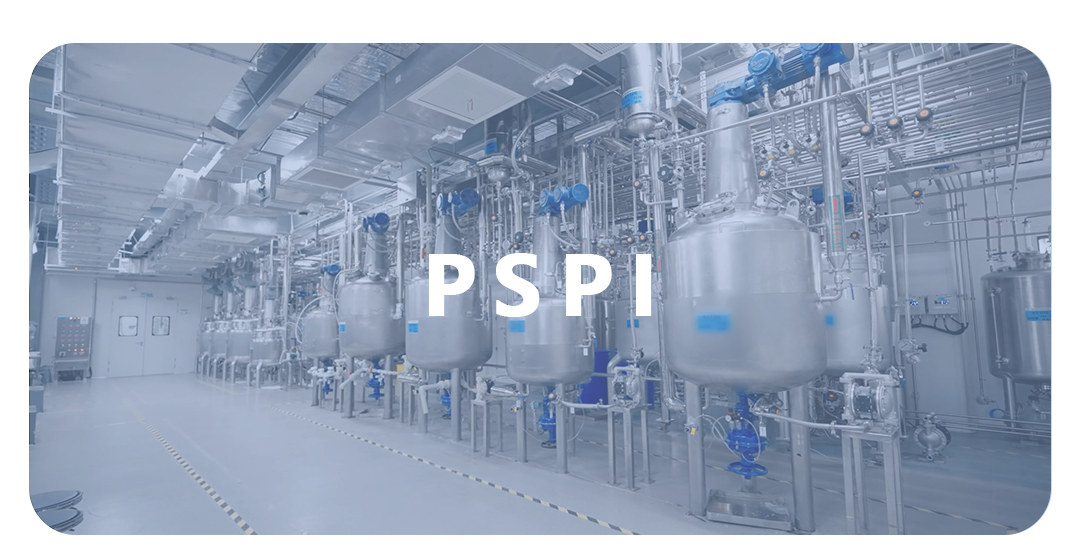
Wafer-Level Passivation Layers (PI/PSPI) are critical materials utilized in Wafer-Level Packaging (WLP) processes. Applied via spin coating and patterned through exposure and development, they form a permanent, patterned protective layer. Following high-temperature curing, these layers provide excellent passivation protection and stress buffering for the chip surface, effectively enhancing device reliability.
CMP Pad is a technology-intensive product that spans multiple disciplines such as polymer chemistry, polymer physics, organic synthesis, fluid mechanics, tribology, and precision machining.
Advanced Packaging PSPI
ArF/KrF
Temporary Bonding Adhesive(TBA)
Wafer-Level Insulating Passivation Layers
CMP Slurry
CMP Chemical
YPI
PSPI
TFE INK